

- MAX881REUB+T - 集成电路(IC) > 电源管理(PMIC) > 特殊用途稳压器
- LTC3675EUFF-1#TRPBF - 集成电路(IC) > 电源管理(PMIC) > 电源管理 - 专用
- MAX6428KRUR+T - 电池管理芯片
- LTC2634HUD-LMX8#TRPBF - 集成电路(IC) > 数据采集 > 数模转换器(DAC)
- MAX6384LT20D7+T - 监控器芯片
- ADE9000ACPZ - 集成电路(IC) > 数据采集 > 模拟前端(AFE)
- MAX6126BASA21+ - 集成电路(IC) > 电源管理(PMIC) > 电压基准
- MAX8841ELT18+T - 集成电路(IC) > 电源管理(PMIC) > 稳压器 - 线性
- MAX4228EUB - 集成电路(IC) > 线性 > 放大器 > 仪器,运算放大器,缓冲器
- MAX1159AEUI+ - 集成电路(IC) > 数据采集 > 模数转换器(ADC)


ADP2311 - Dual 1 A, 18 V Synchronous Step-Down Regulator with Fail-safe Voltage Monitoring
ADP2311是AD公司的一款开关稳压器产品,ADP2311是Dual 1 A, 18 V Synchronous Step-Down Regulator with Fail-safe Voltage Monitoring,本站介绍了ADP2311的封装应用图解、特点和优点、功能等,并给出了与ADP2311相关的AD元器件型号供参考。
ADP2311 - Dual 1 A, 18 V Synchronous Step-Down Regulator with Fail-safe Voltage Monitoring - 开关稳压器 - 电源管理 - Analog Devices
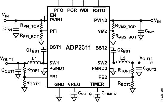
The ADP2311 is a fully integrated, dual output, synchronous step-down dc-to-dc regulator. The regulator operates from input voltages of 4.5 V to 18 V, and the output can regulate down to 0.6 V. Each channel can provide up to 1 A of continuous output current.
The ADP2311 integrates the high-side and low-side MOSFETsto provide a very high efficiency, compact solution. Both channels of the regulator run at 180° out of phase to reduce the input ripplecurrent and the input capacitor size, thereby helping to lowersystem electromagnetic interference (EMI). The ADP2311 also integrates internal compensation and soft start circuitry to simplify the design.
An on-chip watchdog timer can reset the microprocessor if it fails to strobe within a preset timeout period. Accurate voltage monitoring circuitry and a power fail comparator provide a controlled power-up and power-down sequence to enhance system reliability.
The ADP2311 also includes undervoltage lockout (UVLO), overvoltage protection (OVP), overcurrent protection (OCP), and thermal shutdown (TSD).
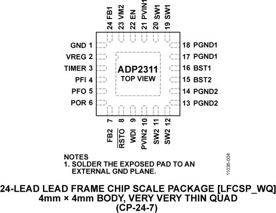
The ADP2311 operates over the −40°C to +125°C junction temperature range and is available in a 24-lead LFCSP package.
Applications
ADP2311评估板是完整的双通道、1 A降压稳压器解决方案,用户可采用近乎理想的印刷电路板(PCB)布局来评估ADP2311的性能。
ADP2311评估板的输出电压针对通道1和通道2分别预设为1.2 V和3.3V。 电源故障输入VIN阈值电压设置为8.99 V。不同的输出和电源故障输入电压可以通过选用合适的无源器件来实现。
产品特性无
- AD9760 - 10位、100 MSPS+ TxDAC?数模转换器
- ADXL326 - 小尺寸、低功耗、三轴±16 g加速度计
- ADP2389 - 集成可编程限流的18 V、12 A降压稳压器
- AD7655 - 低成本、4通道、1 MSPS 16位PulSAR® ADC
- AD7853 - 3 V至5 V单电源、200 kSPS、12位串行采样ADC
- ADR423 - 超精密、低噪声、3.00 V XFET?基准电压源
- AD5660 - 单通道、16位nanoDAC?,内置5 ppm/°C片内基准电压源
- AD5044 - 全精度、四通道、14位、缓冲电压输出、4.5 V至5.5 V nanoDAC?,采用SPI接口
- AD8366 - dC至600 MHz 、双通道数字可变增益放大器
- OP290 - 双通道、精密、低电压、微功耗运算放大器