


- DC2543A - 开发板,套件,编程器 > 评估板 > DC/DC 和 AC/DC(离线)SMPS 评估板
- MAX6315US36D3+T - 监控器芯片
- LTC1709EG#TRPBF - 集成电路(IC) > 电源管理(PMIC) > DC-DC 开关控制器
- LTC2932IF#TRPBF - 集成电路(IC) > 电源管理(PMIC) > 电源控制器,监视器
- MAX7450ESA+T - 集成电路(IC) > 线性 > 视频处理
- MAX1206ETL+ - 数据采集 - 模数转换器(ADC)
- MAX6866UK18D2L+T - 监控器芯片
- MAX11207EEE+ - 集成电路(IC) > 数据采集 > 模数转换器(ADC)
- MAX6724AUTYDD6+T - 监控器芯片
- AD8691AKSZ-REEL - 集成电路(IC) > 线性 > 放大器 > 仪器,运算放大器,缓冲器


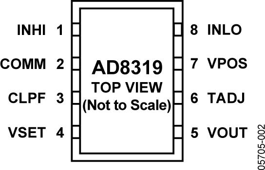
AD8319 - 1 MHz to 10 GHz , 40 dB Log Detector/Controller
AD8319是AD公司的一款RF功率检波器产品,AD8319是1 MHz to 10 GHz , 40 dB Log Detector/Controller,本站介绍了AD8319的封装应用图解、特点和优点、功能等,并给出了与AD8319相关的AD元器件型号供参考。
AD8319 - 1 MHz to 10 GHz , 40 dB Log Detector/Controller - RF功率检波器 - 非RMS响应功率检波器 - Analog Devices
The AD8319 is a demodulating logarithmic amplifier, capable of accurately converting an RF input signal to a corresponding decibel-scaled output. It employs the progressive compression technique over a cascaded amplifier chain, each stage of which is equipped with a detector cell. The device can be used in either measurement or controller modes. The AD8319 maintains accurate log conformance for signals of 1 MHz to 8 GHz and provides useful operation to 10 GHz. The input dynamic range is typically 40 dB (re: 50 Ω) with error less than ±1 dB. The AD8319 has 8 ns/10 ns response time (fall time/rise time) that enables RF burst detection to a pulse rate of beyond 50 MHz. The device provides unprecedented logarithmic intercept stability vs. ambient temperature conditions. A supply of 3.0 V to 5.5 V is required to power the device. Current consumption is typically 22 mA, and it decreases to 200 μA when the device is disabled.
The AD8319 can be configured to provide a control voltage to a power amplifier or a measurement output from the VOUT pin. Because the output can be used for controller applications, special attention was paid to minimize wideband noise. In this mode, the setpoint control voltage is applied to the VSET pin.
The feedback loop through an RF amplifier is closed via VOUT, the output of which regulates the amplifier’s output to a magnitude corresponding to VSET. The AD8319 provides 0 V to (VPOS ? 0.1 V) output capability at the VOUT pin, suitable for controller applications. As a measurement device, VOUT is externally connected to VSET to produce an output voltage, VOUT, that is a decreasing linear-in-dB function of the RF input signal amplitude.
The logarithmic slope is ?22 mV/dB, determined by the VSET interface. The intercept is 15 dBm (re: 50 Ω, CW input) using the INHI input. These parameters are very stable against supply and temperature variations.
The AD8319 is fabricated on a SiGe bipolar IC process and is available in a 2 mm × 3 mm, 8-lead LFCSP_VD for an operating temperature range of ?40°C to +85°C.
Applications
Data Sheet, Rev. A, 3/07
本页提供1 MHz至10 GHz、40 dB对数检波器/控制器AD8319的评估板文档和订购信息。
无
- AD8012 - 双通道、低功耗、电流反馈型放大器
- ADUC7128 - 内置12位ADC和DDS DAC的精密模拟微控制器ARM7TDMI? MCU
- AD8607 - 精密、双通道、微功耗、轨到轨输入/输出放大器
- ADUC7032-8L - 适用于汽车系统的集成式精密电池传感器
- HMC839 - 集成VCO的小数N分频PLL,采用SMT封装,1050 – 1205,2100 – 2410,4200 – 4,820 MHz
- HMC336 - SPDT正控制开关,采用SMT封装,DC - 6 GHz
- HMC461 - 1瓦特高IP3放大器,采用SMT封装,1.7 - 2.2 GHz
- ADL5611 - 30 MHz 至6 GHz RF/IF增益模块
- AD7823 - 2.7 V至5.5 V、4.5 ms、8位ADC,采用8引脚microSOIC/DIP封装
- AD8353 - 1 MHz 至2.7 GHz RF增益模块